Deposition Simulator DEP3D
The simulator DEP3D developed at Fraunhofer IISB allows one to simulate the shape of layers deposited on 3D features as encountered in semiconductor technology. The input as well as the output geometry are given as multi-layer structures which are modified by the deposited layer added on top.
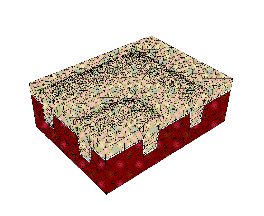
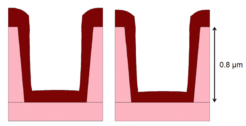
DEP3D provides models for low-pressure chemical vapor deposition (LPCVD) [1], sputter deposition [2], superconformal CVD (Figure 1) [3], and plasma-enhanced CVD (PECVD) [4]. Furthermore, fast geometric operations such as conformal deposition (constant layer thickness everywhere on the structure) are supported. As an example, in Figure 2 the simulation of PECVD is shown [4]. The influence of the position of the contact hole on the wafer has been studied by coupling DEP3D with the plasma equipment simulator Q-VT from Quantemol.
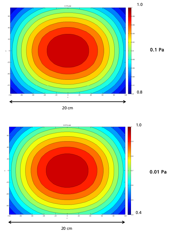
In addition to modeling of profile evolution on feature scale, for physical vapor deposition, the accross-substrate uniformity of the layer thickness and its dependence on the reactor geometry and operating pressure can be simulated (Figure 3).
References
[1] E. Bär, J. Lorenz, 3D Simulation of Tungsten Low-Pressure Chemical Vapor Deposition in Contact Holes, Appl. Surf. Sci. 91 (1995) 321
[2] E. Bär, J. Lorenz, H. Ryssel, Three-Dimensional Simulation of Conventional and Collimated Sputter Deposition of Ti Layers into High Aspect Ratio Contact Holes, in: Proceedings of Conference on Simulation of Semiconductor Processes and Devices 1997 (SISPAD 1997), Technical Digest, IEEE, Piscataway, 1997, p. 297
[3] E. Bär, J. Lorenz, H. Ryssel, Three-Dimensional Simulation of Superconformal Copper Deposition Based on the Curvature-Enhanced Accelerator Coverage Mechanism, in: Copper Interconnects, New Contact Metallurgies/Structures, and Low-k Interlevel Dielectrics, Ed. G.S. Mathad, V. Bakshi, H.S. Rathore, K. Kondo, C. Reidsema-Simpson, Proc. Vol. 2003-10, The Electrochemical Society, Pennington, 2003, p. 21
[4] E. Baer, P. Evanschitzky, J. Lorenz, F. Roger, R. Minixhofer, L. Filipovic, R.L. de Orio, S. Selberherr, Coupled Simulation to Determine the Impact of across Wafer Variations in Oxide PECVD on Electrical and Reliability Parameters of Through-silicon Vias, Microelectronic Engineering 137 (2015) 141